Categories

Archives

PCB VS PCBA: Main Difference, Types, Cost & Quality Basic Standards
By Mer-Mar Electronics | Date posted: | Last updated: December 23, 2022
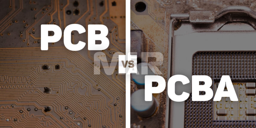
pcb vs pcba

If there are two terms that are often used interchangeably in the electronics industry, they are PCB & PCBA. Yet are they the same? Definitely not! A Printed Circuit Board or PCB as it is popularly referred to is the underlying hardware that is used in electronic appliances. It can also be referred to as a blank or bare board. A PCBA on the hand, stands for Printed Circuit Board Assembly. While a PCB is a blank board, the assembly process ensures that all the components are mounted on it. It is after mounting all the components at the specified locations and integrating the circuits that a functional board is ready.

Let us look at both PCB & PCBA in some detail:

What Is PCB?

These blank boards are the basis of electronic devices and their use is therefore ubiquitous. Made up of fiberglass or composite epoxy they support the components that are placed on them. PCBs, in turn, are of several types:

Three Type of PCBs

1. Single-layer PCBs

These are the simplest type of PCBs that have a single layer of conducting material

2. Double-layer PCBs

These have a layer of conducting material on both the top and bottom of the board

YOU MAY ALSO LIKE: Single Sided Vs Double-Sided PCBs

3. Multi-layer PCBs

They have more than two conductive layers.

What does PCBA mean?

PCBA refers to complete PCB assembly that has all the electronic components in place to ensure effective functioning of the board. PCB Assembly largely uses two methods:

Types of PCBA

1. Surface-Mount Technology

SMT assembly involves mounting electronic components to the surface of the PCB. The steps involved here include:

  • Preparing the PCB
  • Placing the Components
  • Reflow Soldering
  • Inspection

2. Thru-Hole Technology

Through hole assembly is process that involves drilling holes in the PCB. It is through these holes that electronic components can be attached. This makes for strong connections between the board & the components & therefore to durable assemblies. The steps involved here include:

  • Drilling the holes
  • Placing the leads
  • Soldering
  • Inspection

While manufacturing a blank board is easier, as the above process shows, assembly is a fairly complex process that involves placing several components. With miniaturization of boards and increasing component density, the process is even more intricate.

Also, while bare board testing is done by way of either Pinned Fixture Test or Flying Probe test. When it comes to testing of PCBA, there are a wide variety of tests including AOI, AOX, ICT, Smoke Testing, Black Box Testing, Regression Testing and more to ensure that the boards function effectively. Additionally, he boards need to adhere to specific IPC standards for PCB assembly.

Cost of PCBA

There are many factors that affect PCB assembly cost

  • Cost of Bare Board & Components
  • Cost of labor
  • Tooling cost
  • Turnaround time involved
  • Quantity required
  • The technology being used
  • Packaging specifications & more

Material Used in PCB and PCBA

Materials used in PCBs

There is a wide range of factors that lead to the choice of PCB material. Some of these include:

  • Mechanical Strength
  • Thermal Performance
  • Dielectric Constant
  • Temperature Resistance, and more

Types of materials used in PCB Manufacturing include:

1. FR-4

This is a commonly used material that comprises of a glass reinforced epoxy laminate sheet. It is particularly known for its tensile strength

2. Teflon

This is used in high-speed applications that require tight tolerances. That it is very light as well as flame resistant makes it extremely useful.

3. Metal

The use of metals such as copper, aluminum, iron is wide spread, these particularly work well where the PCBA process is done through SMT technology.

Materials used in PCBA

PCB Vs PCBA: Difference Between PCB Vs PCBA

Both PCB & PCBA are steps in the final production that goes into all electronic appliances. While a PCB is a blank circuit board, its assembly with various components leads to a functional board. While manufacturing a blank board is easier, assembly is a fairly complex process that involves placing several components. With miniaturization of boards and increasing component density, the process is even more intricate. In terms of cost also, while it is cheaper to produce a blank PCB, typically assembly of components costs more.

As a handy reckoner, the differences between PCB & PCBA can be summed up as below:

Parameters PCB PCBA
Presence of Components Bare Board with no components Components are mounted
Turnaround Time Is Quick Assembly is an intricate process & takes time
Packaging used Vacuum packing Compartmental anti-static packing
Testing Comparatively less Complex & Stringent testing
PCB
PCB Assembly
PCBa

How does Printed Circuit Board company ensure PCB quality control Methods?

By Mer-Mar Electronics | Date posted: | Last updated: March 20, 2023
printed circuit board company

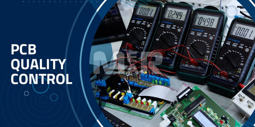
PCBs have a strong role to play in a wide range of industries powering a host of electronic equipment. In addition, they are also widely use in mission-critical industries such as medical, aerospace and others. In such industries, in particular, failure of the product can turn out to have far-reaching consequences. It is imperative, therefore, that the PCB goes through a host of quality control processes to ensure its seamless working.

Here are the many ways in which a every printed circuit board company makes sure to manufacture the quality PCB.

YOU MAY ALSO LIKE: Debunk These PCB Myths to Meet High-quality PCBs

PCB quality control for component procurement

The right components have a strong role to play in the quality of the PCB. In order to ensure this, the PCB manufacturer undertakes the following processes:

  • Validation of BOM

This involves checking for a number of items such as-

  • Verification of manufacturer part number
  • Verification of component reference designator
  • Checking of component manufacturing status

In addition, the other aspects to check for, include:

  • MPN-footprint match
  • Use of a trustworthy supplier so that the components thus procured are genuine.
  • Ensuring that the shipping documents have no errors
  • Visual inspection of components to see that they match your order.
  • Ascertaining solderability
  • Ensuring that the components meet tolerance ranges.

Printed circuit board quality control methods

With these quality control methods, a reputed printed circuit board company ensures that any errors in the PCB are caught early. While this list of tests isn’t exhaustive, it will give you a fair idea of the kind of checks and balances that need to be in place.

Flying Probe Testing

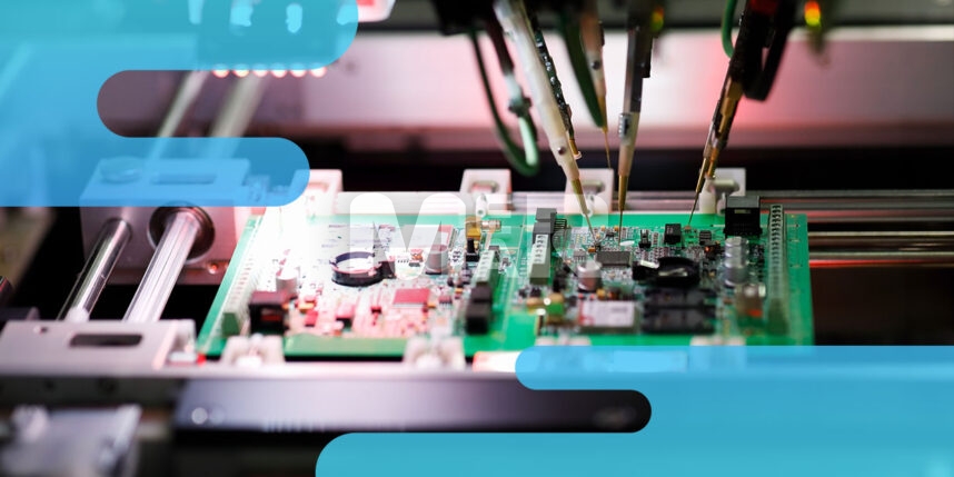
A key component of electrical testing, it makes use of a generic board holder along with probes. It ensures testing for opens & shorts. Flying Probe testing can also perform memory module programming. The fact that it does not require test fixtures & has very little set up time is a big plus in its favor.

Bed of Nails

Also known as an In circuit test fixture, this test comes in handy to check any bad components as well as defects. The test particularly comes in handy in mass production. The big advantage that Bed-of-Nails testing offers is that in identifies specific components that are faulty. It, therefore, goes a long way in improving the efficiency of production as also in reducing maintenance costs.

3D Optical Inspection

Simply put, this is a sophisticated form of visual inspection that makes the use of cameras. The images taken from the camera are then compared with the schematic to determine accuracy. Any discrepancies thus being flagged off it ensures that you do not have to deal with costly errors at a later stage.

Burn-in Testing

It is important to simulate the actual working of a PCB with the requisite stress & load. This is a task that is undertaken by way of burn-in testing. With a burn-in test often power is pushed through a PCB for as many as 168 hours. Burn-in testing thus works very well in determining early failures.

Functional Testing

Similarly, functional testing comes in extremely handy to ensure that there are no issues in powering up of the PCB. The PCB manufacturer can design the test on his own or may follow the specifications shared by the customer.

X-Ray Fluorescence Testing

The European Union Directive on the Restriction of Hazardous Substances (RoHS) holds electrical and electronic equipment (EEE) companies directly responsible for ensuring their products conform to its strict standards and ensure that the products do not contain hazardous substances so notified, above the legal threshold.

This test is therefore important to figure out if any parts contain RoHS substances such as Mercury, Lead, Cadmium and more. In fact, the test focuses mainly on those parts of the product that have the highest risk of containing RoHS substances. Needless to mention that this test is critical to ensure that you do not face any regulatory issues once the product is shipped.

YOU MAY ALSO LIKE: Advantage of RoHS Compliant

PCB Quality Control for Assembly

This stage also involves extensive testing such as:

  • Visual inspection to look for issues such as any unattached components, excess solder & more
  • X-Ray inspection
  • AOI
  • Sawing to inspect vias
  • ROSE testing to determine the cleanliness of the PCB
  • Electrical testing, and more

While it is important that you go with a manufacturer who performs the above tests, in addition to these tests, here are some other things to look for in choosing the right manufacturer who will ensure quality control:

Certifications

It is imperative to look for the fact that the manufacturer is certified by the following bodies:

  • Institute for Interconnecting and Packaging Electronic Circuits (IPC).
  • International Organization for Standardization (ISO). In fact, ISO compliance is especially important for medical devices.
  • FDA Registration. When it comes to medical grade PCBs, an FDA registration also goes a long way in telling you that the manufacturer follows norms with respect to design, production, packaging, maintenance & more.

To sum up

In addition to the above checks, it is also important to figure out if the manufacturer has an internal structure and processes in place that enable them to meet quality standards. One such process is the formation of multi-disciplinary teams that include professionals from different functions who meet periodically to review manufacturing issues as also discuss best practices & trends.

The choice of a professional, reliable printed circuit board company is the first step that you can take toward quality manufacturing. Mermar Electronics is one stop solution for your PCB services. Mermar Electronics is an ISO-9001:2015 AS9100D Certified company since 1999 and provides top-notch PCB services including PCB assembly and PCB fabrication services. Fill out the form below to request a free quote now or mail us at sales@mermarinc.com.

Printed Circuit Board Company

What is the difference between 2-layer and 4-layer PCB?

By Mer-Mar Electronics | Date posted: | Last updated: November 12, 2022
2 layer vs 4 layer pcb

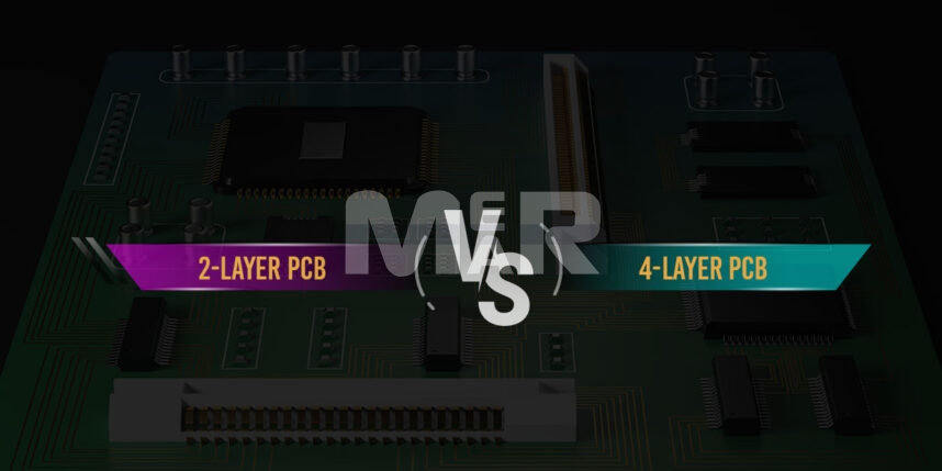
When it comes to efficacy of circuit boards, a number of parameters become important. These range from signal integrity to lack of interference, from complexity of design to cost. While PCBs can range from 2 to multiple layers, each of these come with their own set of strengths. Let us analyze 2-layer vs 4-layer PCB on several parameters of efficiency and efficacy.

2-Layer VS 4-layer PCB

2-Layer PCBs also referred to as double-sided boards have two copper layers with a substrate material sandwiched between them.

The advantage of multilayer PCBs; specially 2-layer PCBs is that they can connect components on both sides. They have holes, also referred to as vias that help connect the circuits. It also has room for a ground grid. In turn, this goes a long way in reducing electrical noise.

4-Layer PCBs have four layers of copper, with the top & bottom layers being signal layers and the inner layers being ground and supply planes. The 4-layer boards also have vias. With the presence of the ground & supply layers, electromagnetic interference is greatly reduced. What it also offers is a short return signal path.

YOU MAY ALSO LIKE: Single sided PCB VS Double sided PCB

1. Difference in terms of stack-up

Largely this comprises of the top layer that is referred to as a signal layer. The layer is 0.0014-inch thick and is made of copper material amounting to about 1 oz.

The 4-layer PCB comprises of the top and bottom layer as also two inner layers. The top or the signal layer made of copper which is 0.0014 inch in width, is followed by a prepeg layer that has a thickness of 0.0091 inch and a dielectric constant of 4.2. The prepeg layer, in turn, is followed by an inner layer, referred to as plane. A core sublayer comprises the inner layer 1 and has a width of 0.037 inch. This is followed by the inner layer 2 which is made of 1oz copper and has a thickness of 0.0014 inch. The inner layer 2 is constituted of another prepeg sublayer that comprises of 2 sheets. Finally, comes to the bottom layer, which is a signal layer as well. Its thickness is 0.0014 inch. When it comes to the interconnects, they are soldered on the top and bottom layers.

2. Difference in terms of Design

As opposed to a single layer PCB, the 2 layered PCB offers a higher surface area. This PCB uses vias to create electrical connections that enable the routing of the traces.

The 4-layered PCB has an even higher surface area than 2-layer PCB. Their design involves having a prepeg layer that can bond 2 or more double-sided boards. The prepeg also functions as a dielectric between layers.

3. Difference in terms of functionality

The 2-layer PCB is known to deliver a high degree of functionality as such PCBs do not suffer from propagation delays. Of course, a 4-layer PCB is preferred with its design comprising of ground & VCC plane layers as well as two signal layers. It’s added functionality, therefore, comes in extremely handy when it comes to complex functions.

4. Cost difference between 2 layer and 4-layer PCB

The complexity of design renders the 4-layer PCB to be more expensive than a 2-layer one. The higher cost of 4-layer PCBs is also on account of the fact that it offers superior signal quality with less distortion.

YOU MAY ALSO LIKE: Factors which affect the PCB assembly cost

5. Difference in terms of lending themselves to prototyping

Needless to mention, that a 4-layer prototype is more complex than a 2-layered one. However, with the use of automated software like Gerber an accurate prototype can be created. The software offers the choice of a number of parameters such as:

  • Thickness of the board
  • Hole thickness
  • Minimum pitch
  • Board finish

It also works well if the prototyping job is outsourced to an experienced contract manufacturer who specializes in creating prototypes.

How to choose between 2-layer & 4-layer PCBs?

Some of the aspects to consider in making the choice, include:

1. Complexity of the circuit

For complex circuits that feature RF circuitry, long digital buses, complex components and connections, 4-layer circuit boards are highly preferred. In such cases, using 2-layer boards would lead to compromise of the signal integrity.

2. Density of the circuit

In terms of circuit density, you could choose any of the boards as both allow for components to be mounted on both sides of the board.

3. Cost

If budget is a constraint, 2-layer boards work better as 4-layer boards that offer high functionality are also higher in terms of cost.

To sum up

The 2-layer and 4-layer boards offer different levels of functionality & work well for different types of projects. Therefore, the complexity of the project determines the choice of the right PCB.

If you are still confused, then contact Mer-Mar Electronics. Mer-Mar Electronics is an ISO 9001:2015 certified company who provides multilayer PCB assembly and fabrication. With the help of a team of experts, Mer-Mar Electronics provides highly durable and reliable PCBs. Request a quote for PCB assembly now to know more about our services.

2 Layer PCB
2 Layer Vs 4 Layer PCB
4 Layer PCB
Multilayer PCB
PCB Assembly

Everything that you should know about PCB In-circuit testing!

By Mer-Mar Electronics | Date posted: | Last updated: November 9, 2022
In-circuit testing

PCBs are highly complex because it’s made up of a large number of components. It is crucial that each of these components performs to its optimal capacity. Any defect in these components can lead to the malfunctioning of the PCB and hence of the electronic device. That’s why testing each component separately becomes very important. This is what in-circuit testing entails as it helps in diagnosing any faults in the components of the PCB.

YOU MAY ALSO LIKE: PCB Components Assembly Process

What is In-circuit Testing?

In-circuit testing helps in testing components of the board individually; so, we can determine faults if it is present in a particular component. An automated test goes a long way in detecting the defect & taking appropriate action. In-circuit testing is conducted in two parts:

  • Power-off tests
  • Power-on tests

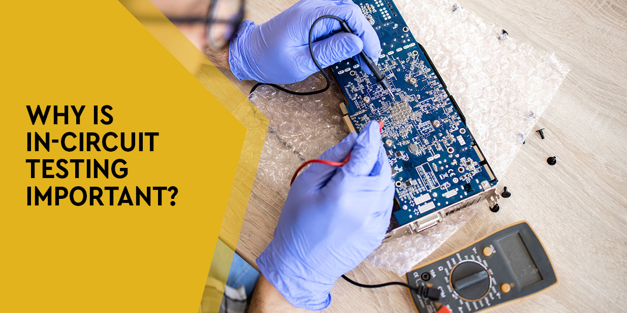
Why is In-circuit testing important?

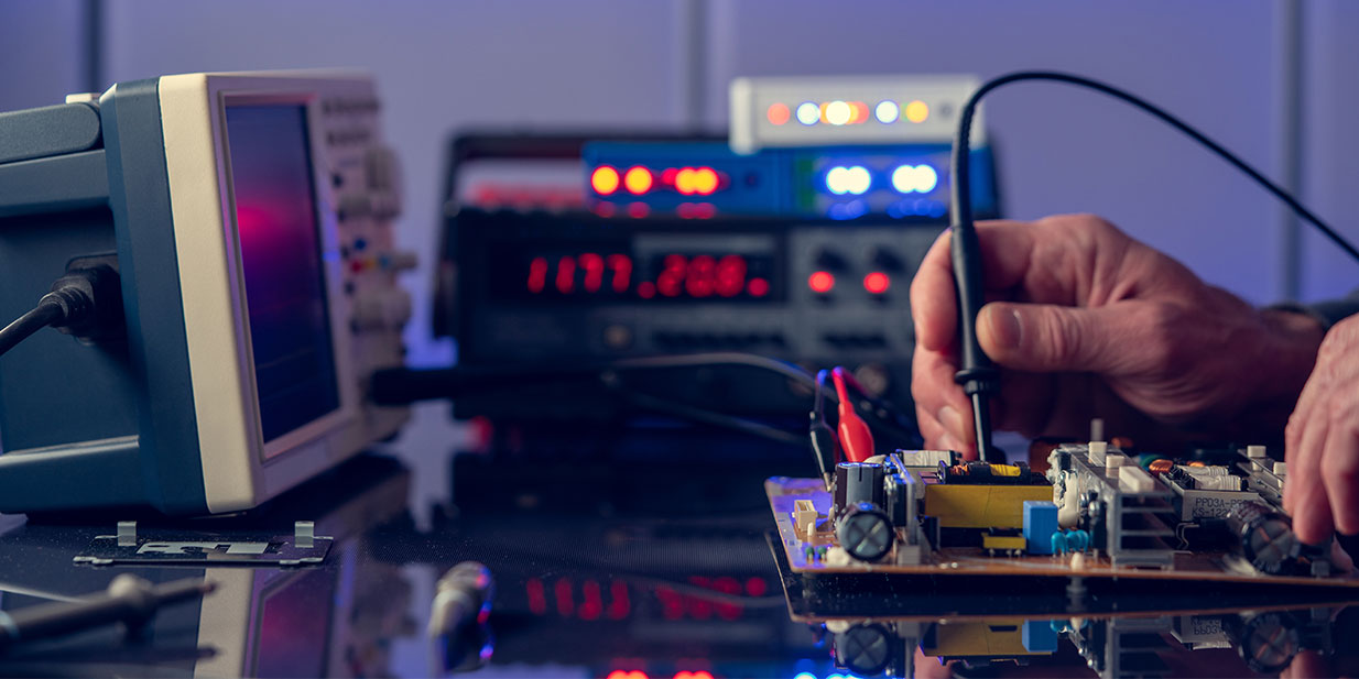
In Circuit Testing PCB

The simple reason for in-circuit testing being so important is the fact that it helps catch errors before they become too costly. The importance of this testing also lies in the following facts:

  • They are easy to program.
  • There is little room for operator error.
  • The testing is quick & reliable.
  • The testing is comprehensive.
  • The results are easy to interpret.

ICT & Fault Coverage Verification

ICT is typically known to find around 98% of faults and therefore is known for its high fault coverage. The reasons why some faults may be left undiagnosed is because:

  • It isn’t always possible to gain total coverage of the board.
  • Low value capacitors can pose a problem.
  • It may not be possible to access all nodes on the board on account of varying reasons such as the tester having insufficient capacity, the tester is shielded by a large component. In such cases implied testing needs to be carried out where a section of the circuit is tested as an entity.

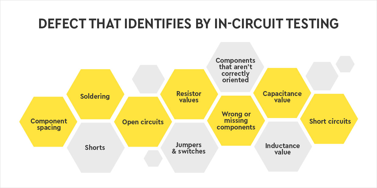
Defect that identifies by In-circuit Testing

In Circuit Testing and Defects

With in-circuit testing, the following parts of a PCB are tested and defects identified:

  • Component spacing
  • Soldering
  • Shorts
  • Open circuits
  • Resistor values
  • Jumpers & switches
  • Wrong or missing components
  • Components that aren’t correctly oriented
  • Capacitance value
  • Inductance value
  • Short circuits

Components in ICT testing

There are a number of in-circuit test systems that are available. Irrespective of the kind that you choose, some components that are common to all ICT testers include:

  • Controller
  • Software
  • Interface
  • Fixture
  • Analog scanner
  • Powered Analog tests
  • Analog Digital Opens

ICT Testing Advantages

ICT offers a wide variety of advantages including:

  • It is highly accurate.
  • It is fast and reliable.
  • It is easy to program.
  • Is economical, particularly when it comes to bulk testing.
  • Ensures high fault coverage.
  • Works well for through-hole assemblies.
  • Does not require high maintenance.

ICT testing disadvantages

Despite the fact that ICT is quite comprehensive, it comes with its own set of disadvantages, namely:

  • In case of small SMT components with high density, this method isn’t too helpful.
  • In case the test pins aren’t in proper contact with the test pads, there will be inconsistency in results.
  • It is imperative that the test pins are cleaned so that chances of failure are minimized.

Different types of In-circuit testing equipment

In Circuit Testing Equipment

Even if the term In-circuit testing is widely used, the fact remains that there are several different types of testers. The choice of testers largely depends upon:

  • The manufacturing/test process used
  • The volume & type of boards

Some of the In-Circuit testing equipment that are widely used, include:

Standard ICT Machine

This offers basic resistance and continuity measurements while also offering capacitance testing as also testing of device functionality.

Check this out: Our PCB manufacuring equipment

Flying Probe

This is found extremely useful as it has a fixture to hold the board. Importantly, contact is made through probes that can move around the board. The fact that there is a software that makes it easy to accommodate any board updates, adds to its efficacy

Manufacturing Defect Analyzer

Popularly referred to as MDA, it offers testing related to resistance, continuity as well as insulation. This test is useful for ascertaining manufacturing defects such as open circuit connections or short circuits

Cable Form Tester

This tester comes in handy to test cables. It works like the MDA, however, in this case, sometimes, high voltage needs to be applied to test for insulation.

In-circuit Testing FAQs

1. What is the difference between dynamic testing and in-circuit testing?

ICT is an example of white box testing wherein an electrical probe tests a populated printed circuit board for its individual components. It helps check for faults such as shorts, opens & more. When it comes to dynamic testing, the board is exposed to high temperatures and input signals are applied to all components of the board so that the exact point where PCB failure may occur, is identified.

2. What is ICT for PCB?

ICT or in-circuit testing helps check a printed circuit board for faults such as shorts, opens, and more. It works by checking errors that occur during fixing components on the board. Essentially, it helps you replace any defective part, easily. Additionally, ICT also help check whether the solders are sturdy as well as the malleable strength of chips.

Mer-Mar Electronics is proud to be one of the reputed organizations offering high-quality PCB assembly services for over 40 years. Our in-warranty rejection rate for assembly defects has averaged below 0.7%. Our consistency in product quality and regular upgradation of the latest tools and machinery is the primary reason we are able to retain our customer base year to year.

PCB Assembly
PCB Testing
Back to top