Understanding Complete PCB Assembly Cost & Factors that Impact the Cost

By Mer-Mar Electronics | Date posted: | Last updated: April 29, 2023
PCB Assembly Cost

In the PCB industry, balancing manufacturing costs and product quality is a huge challenge. You need to identify the expenses involved in each stage of PCB development. There are multiple factors affecting the quality of PCB during fabrication and assembly. Knowing the PCB assembly cost breakdown can assist the designer in choosing the right components for the PCB design. Along with the pricing of the components, features like the board size, PCB material, number of layers, type of PCB assembly method, etc impact the overall PCB fabrication and assembly cost. Further services like testing, packaging, and shipment will add to the total PCB production cost. Collaborating with an experienced contract manufacturer (CM) will benefit in reducing costs and building quality PCB products.

There are some assembly challenges commonly observed during PCB manufacturing. They can be a shortage of components, non-standard PCB dimensions, wrong positioning of the inspection equipment in the assembly line, and many more. In turnkey PCB assembly, your CM will have an excellent network for component sourcing. This helps procure genuine parts at lower prices. It is recommended to add alternate parts to the Bill of Materials (BoM), especially for components that are specific to your board functionality. Choosing a standard PCB size may not be viable in many cases. But both large and small boards can add extra assembly costs. After PCB assembly, it is crucial to inspect the board for any visible placement and soldering faults. Your CM should have the latest assembly setup with optical inspection machines suitably placed in the assembly line. This is essential to increase line efficiency.

PCB Assembly Cost Breakdown

If we break down the various components of a PCB assembly cost, it will be mainly the following four items:

1. Bare board cost

Usually, PCB fabrication and assembly are done together. The cost of bare board manufacturing depends on the material selected, the number of layers, and the board size. You must share the Gerber file and other important PCB design files with your CM for the PCB fabrication.

2. BoM cost

This is the expensive part of a PCB assembly. The bill of materials provides the list of all components and sub-assemblies required for the product assembly. You may have to keep margins for material wastage during the PCB assembly.

3. PCB Assembly cost

The type of assembly technique used determines the labor and engineering requirements of the PCB assembly. Mounting the components on the bare board is a critical process. Surface Mount Technology (SMT) method is commonly used and is cost-effective.

4. Board Testing cost

The assembled PCB must undergo visual inspection and functionality testing. It is recommended to include PCB testing and debug support from your CM. This will save time and assist your CM in improving the assembly line for the next production batches.

It is beneficial to know the various aspects that influence PCB assembly pricing. This will guide you in optimizing the overall PCB production cost.

Factors affecting the PCB assembly cost
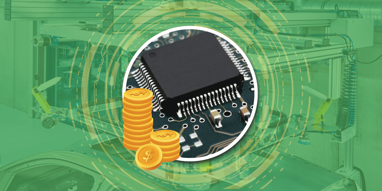
PCB assembly cost drivers

1. PCB dimension and thickness

The assembly cost increases with the board thickness. Drilling holes in bulky boards is complex and involve precise apparatus. Non-standard PCB sizes will require customized assembly panels, adding to the expenses.

2. Lead time

Some CMs can deliver PCB assemblies in just one working day based on the volume and design complexity. But it will be very expensive. You can opt for a longer lead time and reduce the assembly cost with prior planning.

3. Build volume

It is recommended to estimate the product requirement for over a year and then place the assembly service order. High build volumes will be cheaper as the setup charges and one-time expenses will be covered altogether. Many CMs provide good discounts on bulk orders.

YOU MAY ALSO LIKE: Ways to get low-cost PCB assembly

4. PCB Design complexity and customization

Increased board complexity calls for higher assembly charges as it affects the engineering and labor costs. If you require customized PCB assembly like ruggedized PCBs for harsh environments, then the price shoots up.

5. Chosen PCB assembly method

All the latest PCB assemblies are built using the SMT method. But some special circuitries require a Through Hole Technology (THT) approach. This is expensive and suitable for small build volumes. Surface mount parts are best suited for compact PCB designs. If your circuit board is designed using SMT components, then the assembly cost will be drastically reduced.

6. Board and component materials

Choosing the board material is mainly dependent on the circuit functionality. FR4 is the commonly used substrate and is cheaper compared to polyimide material. Electrical components are available in several packages. Leadless packages like BGA or QFNs are expensive. Discrete parts purchased in reels are economical. Your CM can guide you in picking cost-effective components for your PCB design.

7. Coating and Surface finish

To make a PCB corrosion-resistant and durable, surface finishes and coatings are essential. The PCB assembly cost varies with these add-on services. Based on the application, PCBs may require complete or partial surface coatings. The number of coats, coverage tolerances, etc affect the pricing accordingly.

8. PCB Assembly standards and compliance

CMs put in long-term investments to comply with the industry standards like ISO 9001, ISO 13485, and AS9100. Also, assembling RoHS (lead-free) compliant PCBs require a special manufacturing setup. These factors will add to the overall PCB assembly costs.

9. Assembly Technology

Broadly surface mount technology costs lower than through-hole technology. Additionally, some PCBs may also require using ball grid arrays or BGA assembly which impacts the assembly costs.

10. Test and Packaging requirements

Based on the level of testing required for your assembled PCB, the cost will vary. Choosing basic tests like visual inspection and power-on tests may be cheap. But if you require JTAG or functional testing then the cost will increase. Product packaging price increases for EMI sensitive PCBs.

11. Shipment and Delivery

The quick-turn PCB shipments are costly. The delivery schedule directly affects the assembly charges. The labor wages depend on the quantity and schedule of shipment orders.

Conclusion

The above-listed factors can guide you in optimizing your PCB assembly pricing. Your focus should be on the quality of PCB along with cost reduction. An experienced CM can support you in assembling high-performance PCB at a minimum cost.

Opting for Mermar Electronics is the most prudent decision if you desire to avert probable complications, simplify the procedure, and economize on both time and cost. We provide an all-inclusive range of PCB services that entail PCB assembly, fabrication, and design, all under a single roof. To request a quote, kindly fill out the form below, or send an email to sales@mermarinc.com .

PCB Assembly Cost

Top things to check before submitting PCB design & placing online PCB order!

By Mer-Mar Electronics | Date posted: | Last updated: April 13, 2023
Things to check before placing pcb manufacturing order

Building PCBs with a high production yield requires a thorough evaluation of the design and assembly processes. You may have to tick multiple checklists before submitting your PCB design for manufacturing. Adhering to the DFM (Design for Manufacturability) guidelines is crucial. The reliability of a circuit operation depends on the manufacturing processes. If counterfeit components are mounted, the board will fail prematurely adding debug costs to your account. An accurate PCB BoM (Bill of Materials) and an approved vendor list is vital in procuring genuine components.

The PCB material chosen should be based on the operating temperature and the design functionality. During the fabrication process, the physical construction of the PCB impacts its structural integrity. Sharing comprehensive design data with your contract manufacturer can avoid delays in PCB manufacturing. Starting from design to assembly, each stage must meet the necessary quality requirements for building a successful PCB product. You can create a suitable design checklist to verify these critical aspects before handing it over to your CM.

PCB quality checklist can avert possible errors during the design or manufacturing stages. They can track any negligence or unnoticed mistakes in PCB development. The latest EDA tools come with in-built design and layout guidelines that support effective PCB fabrication. If any new component is introduced in the design, it is important to obtain its manufacturer’s datasheet to create a precise footprint. Developing the 3D model and simulating the component placement on the board can avoid assembly issues or respin. We will list out and discuss important checkpoints to consider while you are placing online PCB order and proceed to its manufacturing as a final product.

Things to Check Before Placing Online PCB Manufacturing Order

1. Design Specification

An initial schematics review is done to validate the circuit functionality to be aligned with the design specifications. A DRC (Design Rule Check) is run on the schematics and errors are cleaned. All components used in the schematics should be updated with the latest library files to avoid any placement issues during assembly.

PCB prototype testing reports are analysed and design modifications are completed for the final product. Understanding the end product and its main objectives is the first checkpoint in the PCB design.

2. Component placement and layout verifications

PCB layout involves stack-up design, strategic component placement, and routing. Signal integrity depends largely on the power and ground planes in the stack-up. Logical component placement with enough clearance from board edges is important. Check for visible reference designators on the board for connectors and other main components.

Layout tools can recommend necessary placement and routing requirements for the PCB design. Some of the critical layout guidelines to check before PCB manufacturing are:

  • Avoid 90° trace bends as they can trap residual acid during the fabrication process. This will further etch out copper from the traces and can create open connections.
  • Copper pour near the board edges may cause short in adjacent layers. Maintain enough clearance to avoid such mistakes.
  • Ensure through-hole/ via diameter matches with the board’s aspect ratio. This can prevent production issues wherein vias may crack due to thermal expansion.
  • Check for any void in the thermals used to provide enough heat during soldering. The void can cause irregular soldering during the reflow process and may lead to functional failures.

YOU MAY ALSO LIKE: PCB Component Assembly Process

3. Mechanical dimensions and drill details

Board dimensions and hole/via details should be checked in the Gerber files before sharing with the CM. 3D models of the PCB components can assist in identifying mounting issues, connector mating errors, etc. So, generating 3D models and simulating the assembly is a critical checkpoint before going for PCB manufacturing.

4. Silkscreen and Solder mask

Legible PCB silkscreen is used to identify the components’ location and orientation on the PCB. During the circuit design, it is important to ensure enough spacing between the silkscreen and the component outline. Also, the silkscreen should not be placed on a copper layer without a solder mask as the ink may melt in the solder joints. Follow uniform silkscreen size throughout the PCB design.

A solder mask is applied to isolate the copper traces from incorrect soldering. Applying solder masks in high-density designs is cumbersome. In such cases follow the clearance restrictions to avoid solder bridges. EDA tools can be configured to set the required distance between the solder mask and the surface components. A DRC check and a detailed layout review are mandatory checkpoints before proceeding with the PCB fabrication process.

YOU MAY ALSO LIKE: Solder Mask VS Silkscreen

5. PCB Fabrication checks

A fab drawing provides the manufacturing requirements of a PCB design. It includes the board outline, layer stack up, drill file, title block, etc. It is different from assembly drawing which is used to provide component assembly details. It is important to check that all necessary fabrication data is included in the package.

6. Production file compatibility

Open database (ODB) ++ is the commonly used CAD-to-CAM exchange file format that conveys the required design information to a PCB manufacturer. While a Gerber file alone doesn’t provide complete information, it is necessary to share the centroid (X-Y placement) file, drill file, netlist, and readme text also. IPC-2581 file format and ODB ++ are the intelligent formats for design data delivery. Ensure that your production file package is compatible with your CM’s system.

7. BoM check

Before going ahead with the PCB manufacturing, you must check your Bill of Material for component availability. Look for Do Not Install (DNI) components and obsolete parts in the BoM. Provide an approved vendor list to procure alternate parts for your CM.

8. Obtain Certifications

It is important to acquire all the required certifications for your design before going ahead with bulk production. Based on the end application, list the industry certifications required for your product. Your CM can assist you in getting those certificates.

Conclusion

DFM checklists will help you to optimize your product cost and minimize potential failures during PCB manufacturing. These checkpoints will ensure product quality and high manufacturing output. Neglecting these checks may result in reliability issues and delay in your product delivery.

If you want to prevent potential issues and streamline the process while saving both time and cost, choosing Mermar Electronics is the smartest move. We offer comprehensive PCB services including PCB assembly, fabrication, and design, all in one place. Simply complete the form below to request a complimentary quote or email sales@mermarinc.com .

BOM
PCB Assembly
PCB Order

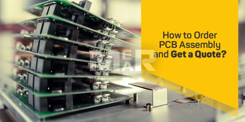
How to Order PCB Assembly and Get a Quote?

By Mer-Mar Electronics | Date posted: | Last updated: February 14, 2023
how to order pcb assembly

With the digitization of the PCB manufacturing process, you can quickly generate a PCB quote online. Based on your requirements, a general cost estimate for PCB fabrication and assembly can be obtained instantaneously.

A PCB quote is thus a document with proposed pricing for the chosen manufacturing services. It can be for PCB design, fabrication, or assembly. The quote offers relevant details on the project’s time, cost requirements, and the manufacturer’s capabilities.

In PCB manufacturing, an accurate quote plays a vital role. The manufacturer can build a successful PCB assembly when the quote includes all the required information. It proves beneficial for both PCB manufacturers and their customers.

By comparing the quotes of different manufacturers, you can easily evaluate their expertise and cost advantages. As the quote is customized for your specific requirements, it reduces the negotiation time and assists in finalizing the order.

As we know PCB assembly is the circuit board mounted with all the electrical components and mechanical fittings. To generate a PCB assembly quote, you must provide the board details, build quantity, component types, and the assembly process required.

Once you obtain quotes from different vendors, you can choose the best service provider based on key factors like domain experience, lowest pricing, lead time, flexibility for changes, and certifications attained.

There are many common PCB problems that you should ensure your PCB manufacturer is avoiding. Ask them how they tackle such problems to choose whether they are good fit for you or not.

How to order PCB assembly?

All PCB manufacturers provide online process to generate a quote for PCB assembly services. It involves simple steps as explained below.

An online form will be available on the PCB manufacturer’s website. You may see several text boxes to enter details and drop-down menus to select an option. The common PCB assembly data required are:

  1. Quantity: This is the count of PCBs to be assembled.
  2. Component sourcing:
    • Kitted – if you are supplying all parts.
    • Turnkey – if the vendor sources the entire list.
    • Combo – Both are sourcing based on available inventory.
  3. Lead Time: Number of days to deliver the PCB assemblies like 5 days, 3 days, etc.
  4. Assembly Part Number: The part number generated for the PCB assembly.
  5. Board type: PCB is in single piece or Panel form?
  6. Assembly sides: Number of component sides to solder. Single or Double?
  7. Lead-free RoHS: Lead-free processing is required or not?
  8. Numbers of through-hole parts: Mention the count of through-hole parts in the bill of material.
  9. Number of surface-mount parts: Mention the count of surface-mount parts in the BoM.
  10. Number of BGA/QFN or leadless parts: Mention the count of BGA, QFN, and leadless parts in the BoM.
  11. Number of unique parts: Mention unique components’ count in the BoM.
  12. Additional PCB assembly information: This can include any assembly-related notes like the type of conformal coating, press-fit connector requirements, firmware loading for programmable devices on the board, X-ray test for BGAs, De-panelling the boards before shipment, etc.

Once you enter the above data and after reviewing your inputs, click on the submit button to send your details to the manufacturer for the PCB assembly quote.

Finalizing PCB assembly quote

You may compare different quotes and finalize on a PCB manufacturer to go ahead with the PCB assembly order. The contract manufacturer will require certain documents and PCB design files to estimate the assembly requirements.

A Bill of Materials (BoM) is the list of all components in excel format. It includes the manufacturer’s part number, quantity required, reference designators, part description, and other significant details for each component used in the circuit design. An approved vendor list is essential to procure alternate parts if required.

Bare board print and assembly drawings are required in a format compatible with your contract manufacturer’s assembly tools. Gerber files provide information on each layer of the PCB stack-up. In the automated assembly process, the centroid file (XY placement file) includes the position and orientation of all surface mount parts. A drill file specifies the location and size of the holes on the PCB.

PCB assembly files are important as they minimize errors by providing accurate information on components’ position, polarity, and mounting instructions. They avoid the ambiguity of silkscreen data and act as a valid reference for manual soldering of through-hole components. They establish effective communication between the contract manufacturers and their customers during the PCB assembly process.

After a review of the documents and finalizing the quote, you can go ahead with the order placement by making the payment. The latest software allows online payment and tracking of your order. You can check the test reports of PCBAs and suggest any recommendations to your contract manufacturer.

Factors affecting the cost of PCB assembly

Knowing the cost influences in a PCB assembly can assist you in optimizing your input to the quote calculator. Various aspects like the assembly type, components used, and design complexity can impact your PCB assembly cost.

  • Though Surface Mount Technology (SMT) is the widely used assembly technique, certain designs require through-hole mounting or a combination of both. Placing all surface mount parts on one side of the PCB can reduce the assembly cost. Since the SMT method is cost-effective and can be automated, choose surface mount parts over through-hole components whenever possible.
  • Opting for a shorter lead time increases PCB assembly costs. For prototypes, a quick assembly is required to prove the concept. But as the design goes for mass production, you can plan the assembly timelines to reduce the cost.
  • PCB features like the board thickness, number of layers, aspect ratio, and surface finish can affect the assembly cost. Following the Design for Assembly (DFA) guidelines can reduce mounting errors and their associated costs.
  • The Non-Recurring Engineering (NRE) charges are applied for one-time services like programming pick and place machines, the inspection process, etc. Features like standard board dimension, optimum PCB thickness, and bulk volume orders can minimize NRE cost to a good extent.

Conclusion

A PCB quote is crucial in choosing the right service provider for your PCB assembly. The online quote has simplified the ordering process and offers the benefit of quality service in set timelines.

After reading the full article, you will find that Mermer Electronics is a good fit to fulfil your PCB requirement. Mermar Electronics provides all kinds of PCB services including PCB assembly, PCB fabrication, and PCB design services. To order PCB quote fill out form below or send mail at sales@mermarinc.com

PCB Assembly
PCB Order
PCB Quote

BGA Package: Different Types & Things You Should Know

By Mer-Mar Electronics | Date posted: | Last updated: January 28, 2023
bga package

Surface mount technology is known for its efficiency when it comes to electronic packages. One aspect that makes for an excellent surface-mount packaging is the Ball Grid Array, popularly known as BGA.

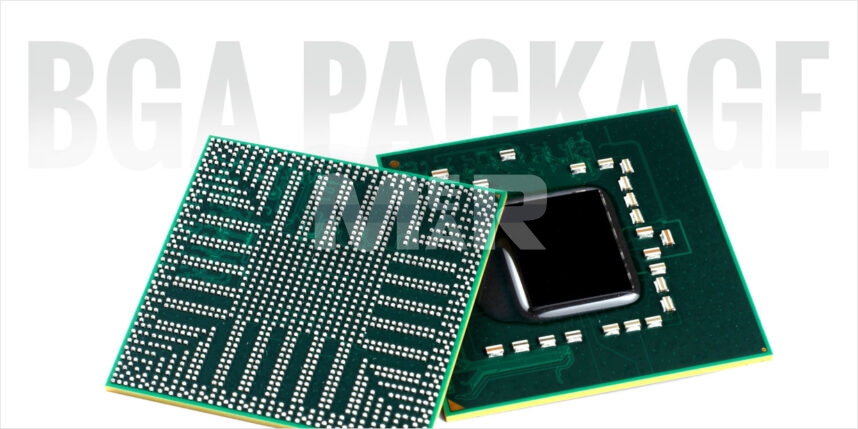
BGA package

Simply put a Ball Grid Array is a Surface Mount Component, which is an array of small conductor balls that come without leads. It is the solder balls that are responsible for passing the electricity from the package to the circuit board. Additionally, the BGA connects to the substrate which connects through wire bonding to the die. Electric signals are thus passed between the balls & the base.

YOU MAY ALSO LIKE: PCB Component Assembly Process

BGA offers many advantages that include:

  • It is quite compact & does not occupy much board space. In a scenario where miniaturization of boards is an increasing trend, its advantage cannot be overstated.
  • On account of its shape, it displays adhesion properties.
  • It is known for its heat dissipation properties
  • It is a good conductor of electricity
  • It is known for its cost-effectiveness

Some aspects to remember while using BGA packages, however, are that:

  • It requires extremely careful handling
  • Post soldering, it is difficult to inspect the solder balls

Types of BGA Packages

There are broadly 3 main types of BGA Packages, as below:

1. Ceramic BGA Package

Here the substrate is made of ceramic. Typically, the solder balls composition includes 90% lead and 10% tin. This kind of package scores in terms of its coefficient of thermal expansion. It has a very high melting point and is known for its thermal conductivity & electrical performance.

2. Plastic Laminate BGA

It was first invented by Motorola and is extremely popular when it comes to double-sided PCBs. Here the substrate is made up of plastic. The other materials involved include Polyimides, dry clad, Bismaleimide triazine epoxy glass. In terms of solder ball composition, it is 63% tin & 37% eutestic lead.

YOU MAY ALSO LIKE: Single Sided VS Double Sided PCB

3. Tape BGA

The advantages that this array offers are multiple:

  • The solder balls have fine lines with a flexible interconnect
  • The chip and heat sink can face downwards. If you choose to do that you need to go with the flip-chip technology. If chips are facing up, wire bond is recommended.
  • It typically works well for thin packages.
  • It is known for its heat dissipation & electrical conductivity.

4. Enhanced Ball Grid Array

Essentially this contains an added heat sink which improved thermal performance. Chips always face down here & wire bond is used for conduction.

5. Flip Chip BGA

The substrate material in this case is BT resin. This kind of array is known for its electrical performance as well as its cost-efficiency.

Typically, the lead:tin ratio here is 63:37, that offers improved surface tension in the melting state.

YOU MAY ALSO LIKE: IPC-j-std-001

6. Metal Ball Grid Array

The substrate used in this array, is aluminum. It is known for both its thermal & electrical performance.

7. Micro BGA

As its name suggests this array is known for its small size & it therefore finds usage in several compact applications. The substrate in this case is packaging tape. It also has an elastomer layer that ensures that there addresses the stress between the tape & the chip.

BGA Package Sizes

Here are some best practices to follow when it comes to BGA package sizes:

  • It is recommended that you use an NSMD pad size when it comes to BGA PCB designs of 0.4mm pitch.
  • If you are using ball sizes of 0.5 mm pitch or less, remember not to reduce BGA pad sizes.
  • When you are using ball pitches less than 0.4 mm, you need to create a bridging between NSMD pads
  • With small pad sizes, solder mask webbings aren’t good enough as adhesive strength is compromised.
  • There should be no traces on the external layers when it comes to BGA pads. On the internal layers, it is recommended to have one trace.

To Sum Up

The advantages of ball grid array for surface mount technology are immense. It is important that you take into account aspects such as weight of the product, heat generated and more, in making the right choice.

Hiring the right PCB manufacturer is also important. Contact Mer-Mar Electronics who have 40 years of experience in the PCB industry, Mer-Mar Electronics Provides PCB assembly, PCB design, and PCB fabrication services under one roof. Fill out the form below request a free quote or send us mail at sales@mermarinc.com.

BGA
BGA Package
BGA PCB Assembly
Back to top