Top things You Need to Know About the Printed Circuit Board Assembly Process!

Electronics have become an integral part of our daily lives – whether it is a smartphone or an electronic component on any automobile vehicle, we have printed circuit boards at the heart of all these electronics. A printed circuit board is nothing about a small green chip covered in metal parts, copper lines, and fiberglass, and held together with a solder mask that is in green.
If you are a beginner and looking for information about the PCB assembly process and its steps, then let’s dive in!
What is PCB Assembly Process?
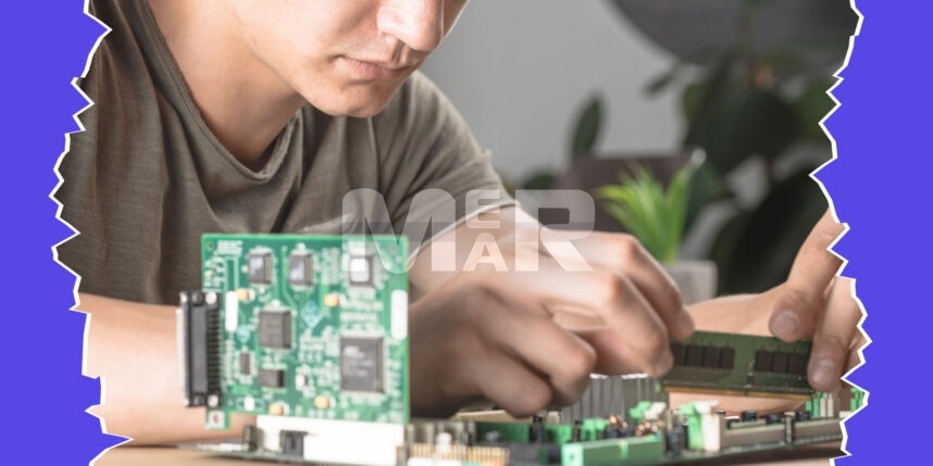
Do you know how these components are stuck on these circuit boards? Do you think they are just ornamental decorations of a PCB board? No, if they are randomly mounted on it, they won’t serve the purpose they are intended for and do not provide the exact functionality. The components have to diligently mounted on the PCB and this process is called PCB assembly.
Here, the copper lines on the bare boards electrically link components with each other. These let the signals run between the features and helps your circuit board function in the designed way. You may accomplish simple or complex functions and can go for smaller to complex PCB. There are single-sided, double-sided, and multilayer PCB assembly and you need to go through multiple stages of deployment in the PCB assembly process.
PCB assembly process is an integrated process that all the stages are important, and we need to flow from one phase to the next till the final stage. Quality also remains the core of the PCB assembly process. You can rely on several manual and automated steps to complete the PCB assembly process.
YOU MAY ALSO LIKE: Factor That Slow Down PCB Manufacturing
PCBA Process Overview
Solder Paste Stenciling
This is the first step of the PCB assembly process where the solder paste is applied to the circuit board. The assemblers apply the solder paste where the parts would sit on the finished PCB. Solder paste is a grey substance that has tiny metal balls with 96.5% tin, 0.5% copper, and 3% silver. It is mixed with a flux that is designed to help the solder melt and bond to the circuit board surface.
You need to make sure that this is applied at the right places on the boards accurately and in the right amounts. You can use a machine for spreading the paste across the stencil for even application.
YOU MAY ALSO LIKE: Our Guide On – j-std-001 Soldering Standard & Requirements
Pick and Place Machine
Once you are done with applying the solder paste to the PCB board, the next step in the PCB assembly process is the pick and place machine that places surface mount components onto the circuit boards. Earlier this was a manual process done with a pair of tweezers. Now, a shift has happened, and this is an automated process that helps in achieving the level of accuracy and consistency that wouldn’t otherwise be achieved.
This indefatigable pick and place machine does the job by picking up the circuit board with a vacuum grip. The robot orients the PCB and begins to apply the SMT on the PCB. Finally, the components are placed on the soldering paste in the preprogrammed locations. Solder paste ensures a tight grip of the components and keeps them firm without any shakiness. There are some machines that add glue during the PCB fabrication phase for a firm grip.
Reflow Soldering
Once the surface mount components are in the right place on solder paste, you need to make sure they remain in there. For this, the solder paste has to be solidified sticking the components to the board which can be accomplished through the reflow soldering process.
The PCB boards are then passed to a conveyor belt that moves through a large reflow oven. The conveyor belt has a series of heaters for heating purpose wherein the temperatures can go as high as greater than 200 degrees Celsius. This melts the solder, and the PCBs move through a series of cooling heaters for letting the solder to cool. The solder also gets solidified and creates a permanent solder joint connecting components to the circuit board.
Once you have the components on the PCB, you can now pass the board through a wave soldering machine. Here the machine has its own solder and some of the PCB Assembly manufacturer prefer using a reflow oven.
YOU MAY ALSO LIKE: Reflow Vs Wave Soldering
Quality Control and Inspection Process
The PCB assembled boards should be tested for functionality and quality purpose. During the reflow process, the movements result in a poor connection and poor quality. Sometimes, even the components can be misplaced. These errors and misalignments will be inspected through a series of tests like –
Manual Inspection
Manual inspection of the PCB board functionality and quality through a visual inspection process by the designer is one way to ensure the quality of your PCB. Of course, as the number of boards increases, this process becomes impractical. This may result in optical fatigue and result in less accurate inspections.
Automatic Optical Inspection
If you have larger batches of PCBAs, you can go for this inspection machine. It has a series of high-powered cameras that are arranged at different angles to inspect PCBs and the solder connections. The AOI machine recognizes the low-quality solder easily and in a relatively short time.
X-ray Inspection
Used in more complex and layered PCBs. It helps to view through these layers and identify any potential hidden issues. If there is any malfunctioning, it will be either reworked or scrapped.
Once you made sure that the functionality is as expected, next test the PCBs for quality.
Through-hole component Insertion
Your PCB board may also include through-hole components that are placed on the board by drilling holes for passing signal from one side to the other side of the PCB.
Types of Soldering Methods Used in PCBA
Manual Soldering
Inserting one component into the designated through-hole. Once it is done at one station, it is moved to the next station, where a new component would be inserted. The cycle repeats till you finish the fitting all the components.
Wave Soldering
In the wave soldering, a conveyor belts runs through an oven. Here, a wave of molten solder moves to the bottom of the board where all the solder pins are placed. If you have a double-sided PCB, soldering the entire PCB would make the delicate electronic components useless.
Final Inspection & Functional Test
Finally, the PCB has to go through functional tests and final inspections. The tests put the PCB through simulating the normal situations in which the PCBs usually operate. The PCB fails the test if there are any unacceptable fluctuations or goes out of the range. The failed PCB either be reworked or scrapped.
Conclusion
Now that you are aware of a little about the PCB assembly process, you need to focus on finding the right partner for your PCB assembly process. Mer-Mar Electronics is a premier Printed Circuit Board assembly provider. You can rely on us for end-to-end PCB assembly process and be assured of high-quality and high-performance.
We are an ISO-certified company and ITAR compliant manufacturer who have been striving to deliver the best RoHS Compliant PCB Assembly services for over 4 decades. We have the capabilities to handle single-sided or double-sided, SMT or through-hole. Mer-Mar Electronics can be a reliable partner for the PCB assembly process right from the start till the finish line.
Get a quick PCB Assembly quote!


