Tips to Overcome the Factors That Slow Down PCB Manufacturing
By Mer-Mar Electronics | Date posted: | Last updated: January 13, 2023
Factors That Slow Down PCB Manufacturing

Printed Circuit Boards are becoming ubiquitous in today’s environment where we tend to use enough and more electrical devices in many aspects of our lives. Circuit boards containing the complex circuit array that they do, both their design and quality is of tremendous essence when it comes to the efficiency of the final product.

Complexity of printed circuit boards also increases their chances of failure on account of factors such as oversights in design, errors in drilling, over etching and more. In today’s highly competitive market where go to market time is of essence in the success of your product, you certainly cannot afford to lose time. Each error and potential failure of the PCB can in turn cause costly delays. What you need, therefore, the right PCB partner who can offer you quick turnaround times without compromising on quality.

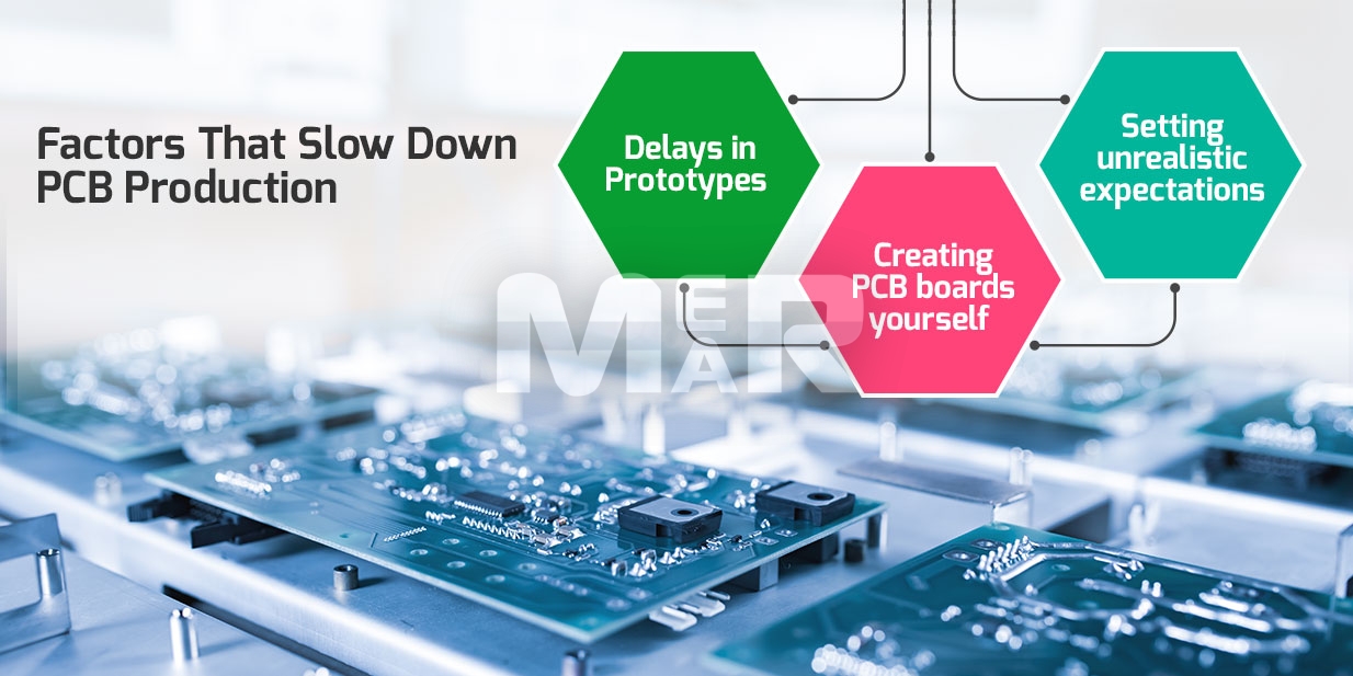
Factors That Slow Down PCB Production
Reason behind your slow PCB manufacturing process

A close look at some of the common factors that can slow down the PCB manufacturing process is imperative so that you can keep these factors in mind in choosing the right partner. Here is a handy checklist that you can refer to while making your choice:

1. Delays in Prototypes

If you are setting out on a new business or expanding your product line, the one thing that you need for sure is a prototype. For the same you need to work with a company that has a quick turnaround time when it comes to developing prototypes. Not only do you need a manufacturer that can provide you these prototypes without delay, you also need someone reliable who can understand your requirements and deliver a prototype that is as per your requirements. Delay in receiving the prototype or receiving a prototype that does not meet your requirements can equally lead to a whole lot of delays down the line that slow down the manufacturing process.

It is imperative therefore that you choose a PCB partner who has a proven track record when it comes to both delivery time as well as understanding your exact prototype requirement. Only with such a partner can you be sure that the prototype will work the way it should and therefore your timelines will not be jeopardized.

YOU MAY ALSO LIKE: PCB Manufacturing Tolerances

2. Creating PCB boards yourself

Given the fact that you could experience delays in receiving prototypes from some PCB partners, you may often be tempted to create PCB boards yourself if you have some amount of technical knowledge. This approach, can lead to a host of costly mistakes besides consuming a lot of your time, which could otherwise be used in other productive aspects of business. The net result could therefore still be delayed time to market. Spending some time to research a partner who is extremely professional and can deliver PCB boards on time and with accuracy is therefore a productive means of avoiding delays.

A professional partner will take a number of factors into account at the design stage itself. These include proper placement of products which if not done correctly can among other things lead to overheating. In fact, the risk of creating PCB boards yourself, is often burned components. Also, with a quality partner, you can rest assured that the components that are used are of high quality and that traces and pathways are in order. There are a whole lot of issues that need to be kept in mind such as proper PCB soldering process, sufficient board thickness, and more which the PCB partner on account of his vast experience will be privy to, but which you may not be exposed to and therefore could easily miss.

3. Setting unrealistic expectations

Another aspect that is known to slow down PCB manufacturing sometimes lies not so much with the PCB partner but in the fact that one tends to set expectations that aren’t realistic. These expectations may be by way of cost of the product or turnaround times. It is imperative that you undertake through research so that you set expectations that are not out of sync with reality. This will in turn help you in creating a product roadmap that will be sustainable.

On the other hand, on occasions you could also come across PCB partners who might offer you turnaround times that seem extremely appealing but which are at the same time, unrealistic. With your research in place this should raise red flags as in case you go ahead with these unrealistic expectations you are likely to meet bottlenecks on the way that could derail your entire plan.

If there is one common learning thread running through the checklist, it is the fact that enough time and energy should be spent on doing thorough research on doing thorough research on the credentials of the PCB partner so that you can consciously avoid these bottlenecks.

Want to Get Your PCB Assembled from Mer-Mar Electronics? Send us inquiry to Get a Quick Quote based on your custom requirements.

PCB
PCB Manufacturer
PCB Manufacturing
PCB Manufacturing in USA
PCB Manufacturing Services
Printed Circuit Board Manufacturing
US PCB Manufacturing
USA
USA PCB Manufacturing

How 5G Fosters the Demand of Advanced PCB Manufacturing?

By Mer-Mar Electronics | Date posted: | Last updated: December 24, 2021
advanced-pcb-manufacturing

The demand for compact devices that are a perfect mix of form and function has forever been on the rise. More so, when it comes to smart phones, which is a highly competitive industry and where success or failure of new generation phones determines company fortunes. Compact smartphones not just mean ease of use to the end consumer they also facilitate use of larger batteries, high-resolution displays and more.

So far PCB manufacturers have been able to solve the form-design conundrum by using high-density interconnects (popularly known as HDIs) which allow enhanced function per unit area as compared to conventional PCBs. HDIs help leverage fine lines as well as laser-drilled vias and therefore have helped in the evolution of smart phones in their ongoing miniaturization.

However as we move from 4G to 5G compatible smartphones, the entire approach to PCB manufacturing needs to evolve. One challenge is to cater to millimeter-wave frequencies, which so far were almost exclusively used by the military. However 5G devices have made them accessible to billions.

Within the 5G smartphone, there needs to be a tremendous increase in the processing power needed to support the huge volume of 5G data. In turn, this is also likely to impact battery capacity among other things. Odds are, therefore, that the space available for HDI PCBs will be severely impacted. Also there needs to be the highest degree of precision in setting thin PCBs as there can be the risk of degradation of signal.

The answer to these issues can be the use of mSAP or a modified semi-additive process. With the use of mSAP, 5G smartphone manufacturers are able to achieve the desired device density without the fear of degradation of the signal. With current space requirements having reduced, mSAP allows 5G smartphone manufacturers to ensure that there is seamless operation at high frequencies.

The way that it works is that a thin copper layer is coated onto the laminate. This is an additive process as it is plated in the areas where the resist is not applied. The copper that remains in between the conductors is then etched away. The difference in this process is that while in the conventional subtractive process, the trace geometries are chemically defined, here the defining process happens through photolithography, which calls for greater precision and lower signal loss. Also in the subtractive process, the treatment that is used to etch the lines vertically, oftentimes also dissolves the copper horizontally as well. This can result in a wedge-shaped trace, that in turn can lead to a number of anomalies.

With the use of mSAP, PCB manufacturers can overcome all the hurdles that are a part and parcel of using HDI. However, the important thing is to implement mSAP in a manner that production is maximized and costs are kept at an optimal level so that the return on investment is maximized and production efficiencies maintained.

One way to ensure that production efficiencies are not compromised is to invest in advanced manufacturing tools that offer competitive advantage. To this end, direct-imaging systems are being increasingly used that ensure 10-15 micron line spacing is achieved. In turn this can result in high accuracy and enable advanced localized-registration features.

Direct- imaging (or DI systems as they are popularly called) and multi-wavelength light sources result in consistent uniformity as well as high quality. Additionally, through the use of advanced automated-optical-inspection systems any defects can easily be identified and quality assured. Also with the use of 2D metrology, the assessment capabilities can be further enhanced. Its use can ensure that top and bottom conductor widths are maintained and proper sampling techniques are used.

It is also advisable to use automated- optical-shaping (AOS) systems as these go a long way in identifying opens, shorts and other such defects. With the use of AOS systems, the need for manual repair can be taken away as AOS provides for far greater accuracy than manual repair. In fact not only is it more accurate, it also eliminates PCB scrap. With so many advanced HDI manufacturing solutions available, it is imperative that they are all connected via a software so that every touchpoint is taken care of and troubleshooting is easily facilitated.

With the evolution of 5G smartphones, there is certainly a need for advanced PCB manufacturing which can take into account an increased density of the embedded electronics while at the same time ensuring that there is no signal friction. With mSAP these specifications are met while technologies such as DI, AOI, AOS and more go a long way in both maximizing yield as well as keeping costs under check. As new generations of smartphones evolve, mSAP is likely to become the mainstream production process. It is not a surprise then that mSAP technology is slated to become the key investment project for PCB manufacturers.

Get a Free Quote for PCB manufacturing!

5G
HDI PCBs
PCB
PCB Manufacturer
PCB Manufacturing
PCB Manufacturing in USA
PCB Manufacturing Services
PCBs
Printed Circuit Board Manufacturing
US PCB Manufacturing
USA
USA PCB Manufacturing

Ways To Avoid On Board Noise In High Speed PCB’s

By Mer-Mar Electronics | Date posted: | Last updated: November 25, 2022
PCB Noise Reduction Technique

In this modern world of digitalization, speed is the prime and basal factor that adds up to product performance at large. Herewith, the multitude of electronic designs is stuffed with a lot of high-speed interfaces in addition to the intensified signal speed that the layout and traces of the printed circuit board act as the fundamental foundation element of the system performance as a whole. The rising enrichment in electronic innovation has resulted in increased demand for high PCB manufacturing and PCB Noise Reduction Technique. Noise on the printed circuit board is the chief deterrent to the overall system performance. This blog highlights the ways and means to reduce onboard noise in high-speed PCBs.

The PCB design ensuring a level of up-gradation in delivering reliability should set out low level and nominal on-board noise in the PCBs. Acting as a prime vital stage to get a tough, noise free, high-performance PCB assembly service, PCB designing is in the mainstream. For this, the factors of significant concerns include effective circuitry design, issue of interconnecting traces, parasitic components, decoupling and grounding techniques for effective PCB Designing. Above all leads the sensitive structuring and mechanics of the traces- The ground loops and ground noise, stray capacitance, high circuit impedance, transmission lines and embedding traces. For the high frequency requirements that have fastest signal speed in the circuitry, the PCB design aspects should involve the above-mentioned significant concerns for a reduced level of noise that in turn gives a durable high-performance PCB solution.

PCB Noise Reduction Techniques

Noise in PCB may adversely affect the PCB performance with the fluctuation induced in the voltage pulse and in the shapes of the current. Take a read to the few preventive steps on avoiding the blunders that can help in enhanced functioning and put a stop to noise in the high-speed PCB.

1. Reduce Crosstalk

Crosstalk is a superfluous inductive and electromagnetic coupling between the wires, traces, cable assemblies, and elements related to electromagnetic field distribution. Crosstalk significantly depends on the technique of routing traces. There is a reduced chance of crosstalk occurrence when traces are routed side by side. In case the traces are routed parallel to one another, it is more likely to initiate crosstalk if the trace segment is not kept short. Other ways to avoid crosstalk are the reduced dielectric height and wider space between the traces.

2. Strong Signal- Power Integrity

It is prudent for the PCB design expert to cautiously consider the Signal and Power Integrity mechanism along with the analog features of the high-speed PCB design. One of the key design concerns for high-speed SI is the right selection of the transmission line for the PCB design depending on the requirement of the exact signal speed, the driver IC and other design complexities that can help to avoid onboard noise in PCB with rapid signal speed. Power Integrity (PI) also acts as a vital part in achieving the required protocols of high-speed PCB design with reduced noise and a constant level of stable voltage across the chip pads.

3. Prevent Cold Solder Joints

The inaccurate welding process can cause cold solder joints. Cold solder joints can cause problems such as erratic cut outs, static noise and much more. Well! To prevent such issues, make sure there is proper heating of the soldering iron at the right temperature. The tip of the soldering iron should be placed on the solder joint to heat it properly followed by the solder application on the joint. You will witness a melting at the right temperature; the solder completely covers the joint. Other ways to improvise the soldering method is by using the soldering flux.

YOU MAY ALSO LIKE: Wave Soldering VS Reflow Soldering

4. Reducing PCB Emissions for Low Noise PCB Design

The adjacent pair stack-up layout is the most desirable circuit layout option to avoid on board noise in PCB. Other prerequisites to get a low noise PCB design with reduced PCB emission includes low chances of splits, add a series termination resistor, use of decoupling capacitor, draw apart the analog and digital ground planes and segregation of the I/O area coupled with the off board or signals on the circuit board that well suit the need of low noise high speed PCB.

It is uncertain to virtually design a noise free PCB with implementing all the above mentioned techniques completely with keeping in mind the requirement of the specific design customization for any PCB project. In order to have plenty of design options to get a noise free PCB within the EMS specifications is why we have presented multiple ways to avoid onboard noise in high speed PCB.

Low Noise PCB Design Manufacturer

One of the California based industry leaders, Mer-Mar Electronics is a highly experienced professional in offering quality PCB with improved performance in PCB design, PCB prototyping, PCB manufacturing and Assembly services. For every time you order, our team of PCB engineers strives to put the whole and soul of their expertise in the circuit board design that best suits the PCB requirement of the client. A noise free high speed PCB manufacturing is our specialized range of service tendering to the PCB requirement of the varied dominant industry verticals. Get in touch with to know more about PCB Assembly capabilities that deliver high speed low noise PCB’s. We welcome you to give us a call at 760/244-6149 or drop a mail at sales@mermarinc.com with regard to your queries. Get a quick quote for High-Speed PCB!

California
High Speed PCBs
High Speed Printed Circuit Board
high-speed PCB
PCB
PCB Assembly
PCB Manufacturing
USA

High Speed PCB Assembly Sway A Whirlwind Of Innovation In Guitar Pedal Board Manufacturing

By Mer-Mar Electronics | Date posted: | Last updated: December 24, 2021
guitar-pedal-board

The present world of catchy, poppy tunes with a unique transformation in the composition of melodies, carols, jingles, jazz, acoustic, rap, rock and many other music pieces gears up a tremendous wave of electronic revolution in the music instruments. Among all, Guitar sets a notion of trendy series of rhythmic modulation in the pedal board with high speed PCB Assembly technology. By this means, the Guitar pedal board manufacturing also lead great contribution in delivering clean and effective classic, vintage and hard rock music in the home environment to concert, small venues, studios and at the professional stage. This article brings into open, the recent innovations in ‘stomp boxes’ or electric guitar pedal boards with the help of custom-build printed circuit board assembly services.

The innovation happened last year and in the upcoming days of 2018 have a series of sensational release of guitar pedal boards that hit the market with a saga of musical flairs. With the emerging boutique and pedal board companies crafting classy electric stomp boxes, the fun doesn’t end with just an electric guitar. The fun lies in the modular synthesis to orchestrate the rhythmic sounds. Nowadays, with the use of zero defect PCBA technologies like Surface Mount PCB Assembly, Through-Hole PCB Assembly, PCB Prototype Assembly and Mastering Mixed PCB Assembly, the leading guitar pedal smiths in the industry has modified the new version of the guitar effects pedal into a ‘Multi Effects Pedal’ that has varied mode, effect and control being featured in one multi effect processor with smooth access to create a unique music composition.

The pedal effect having multi-feature like an analog, harmonizing and pitch shifting mechanism gives a special call out to user friendly guitar pedal board design that are capable to release new planes of music to play for the guitarist. Such creative modulation in the stomp boxes has become a trend setter versions with high quality Complete PCB Assembly. The Smallest Components and Fine Pitch PCB Assembly has bought the new edition of the distortion pedal in a miniature form that makes it much compact layout with extra pedal effects avoiding the unwanted niggle bass in between the tunes. The multi layered, double sided, complex, surface mount PCBA innovates the pedal patch bay with smooth swapping of effects in the instrument and turns out into a patchable module from the effects pedal rig that makes it possible to get the most out of the stomp boxes.

Also, the custom build guitar pedal board assembly was of much in use for the recent modification in the rigs to make them highly capable, sturdy and durable that delivered improved performance in the complex and specialized effect pedal requirements. In addition to these, the smart Pedal Board PCB Prototyping has made it very much possible to give a touch of sophistication in the Reverb pedal, Octavia pedal, Chorus pedal, Wah pedal, Tremolo pedal, Digital delay pedal and more with tech savvy effects such as a switch that rebounds the given sound into same music vibes, the Send-Return FX loop directly switches over to another effect through the same pedal straightaway.

The ongoing research and development in high performance PCB manufacturing and circuit board assembly makes it possible to shape up the electric guitar in a smart and artistic layout that consist of panels with a forward slope having a smooth input/output circuit connectivity with extra pedal slots for future up-gradation of the stomp box modelled with fine structure that easily drains out the unwanted components when in contact with harmful external bodies like liquid, moisture and other harmful stuff. The pedal boards in current times are fabricated with PCB assembly service in compliance with the UL safety standards that match improved quality and security in installing high performance extensions, adaptor and power connection cords.

Simple wiring structured with strong cable routing for standard connection in the stomp box gives a great style to innovate the guitar pedal boards with effective rig requirement of more than four expansion slots. For such type of modified versions, the guitar pedal board manufacturers made sure to go an extra mile and get best Pedal Board PCB technology that introduces the new editions in guitar stomp boxes-making it a great success in the music industry. As per specific pedal board demands, the PCB experts used BGA/Micro BGA, SMT, Thru-Hole, Box Build, Cable harness assembly and rigid/flex PCB assembly capabilities to give a complete blend of creativity, security, audio clarity, rigorous strength with increased quality in the modulation effects that translated the creative idea into real music piece.

For specific demand and switching requirements the modernization is addressed in Production PCB Assembly that has restructured the sound temptation with a frequency knob setting the frequency rate with the help of a voltage controlled oscillator and volts knob setting a balance in volume of circuitry that is at the mainstream in the fuzz pedal. Lastly, the Tailor-made PCB Assembly techniques also targets the hues of tuneful transformation in the keyboard amplifier, loud speakers, guitar amplifier, theatrical equipment, home theatre system, digital audio player and many other consumer electronic sound systems.

Mermar is one of the highly experienced ISO 9001:2008 Certified PCB Assembly and PCB manufacturing professional that specialize in profound implementation of PCB assembly techniques focused with high end customization proving to be the first choice for smart guitar pedal board manufacturing. Team of experts at Mermar tweak a unique version of pedal boards, audio amp music instruments and theatrical equipment that demands varied modulations, neat connections, light-weight, tough and sleek features finely tuning out a perfect sound that a musician had actually imagined. Explore our guitar pedalboard assembly services for more information. We welcome you to give us a call at 760/244-6149 or drop a mail at sales@mermarinc.com with regard to your queries, PCBA consulting or to Get a quick quote for PCB manufacturing and Fabrication!

Best Guitar Pedal Board
guitar pedal board
guitar pedal board assembly
Guitar Pedalboard
PCB
PCB Assembly
PCB Assembly Services
PCB Manufacturing
PCBa
pedal board assembly
US PCB Assembly
USA
USA PCB Assembly
Back to top