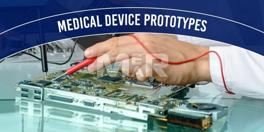
Best Practices for designing Medical Device Prototypes!

If you are developing and manufacturing electronic devices, then don’t make the mistake of ignoring the design aspects of it. Quite often, we see that design for manufacturing (DFM) takes a backseat without any regard for the long-term consequences. Don’t think of cutting down the costs while working on designing the prototypes. It is found that products without design often take a longer lead time and are of lower quality when compared to the products that are designed.
If you are a novice PCB manufacturer and wondering how to get your design prototype for a medical device right, then you are at the right place! Of course, some of the design tips and practices provided in this article are meant for mature designs as well and not limited to medical device prototypes.
Be open to Modifications
Don’t be ambitious and over-confident of getting everything right in the first spin. Things are bound to go down but that’s the only way to abandon that doesn’t work and find the one that works. Ensure all the traces are accessible from the top layer for it is easy to cut, scrape the solder mask, and easy soldering. Make the Vias and test points large enough to easily solder jumpers to these if required. If these are placed too closely, it makes it difficult to modify, and hence some extra space between the components is required while you are designing the layout itself.
Flush out the problems early on
Medical devices are heavily regulated, and you need to be sure of the compatibility issues as you keep adding the components one after another. Even if it’s too early to test the board, you need to give the head start for flushing out the problems at the inception stage itself. Once you have the design prototype, you can look for any issues that rolled out accidentally onto the board. It is better to design in parts rather than populating it with total disregard to the early-stage testing. Remember, it’s the best to nip the issues in the bud itself before they cause chaos later.
Get ready for Multiple Iterations
The design cycle involves heavy consultations with many mechanical engineers and electrical designers. They would be aware of all the constraints of a PCB design. Often, they propose a board outline and your in-house team can hash out the possibilities and rearrange the components, connectors, and placements. You can tweak them, give the final touches, and throw them back to the design team to understand the feasibility issues. This process involves multiple iterations and also relies on accurate 3D modeling of the board, connectors, and wiring.
Ease of PCB Assembly & Serviceability
You may be paying attention to a myriad of trivia, but certain simple things tend to slip out of your mind. Your meticulous routing and placing of components are convenient for everyone? Can a human reach into the assembly and connect them to the cables? Do pads connect to the ground fill ease solderability with thermal relief connections? Can you easily export a 3D model of the board for virtual testing? How about the placement of the components? If you screw up any terminal blocks for connectors it is going to be a nightmare. You need to unscrew every terminal and remove everything for debugging purposes.
PCB Component Placement
Does your contract manufacturer use automated equipment? Do they on conveyors and fixtures for transporting products through the process? Good design practices include spacing between components. They shouldn’t be close to the edge of the circuit board. Also, avoid odd angles. By following them, you can avoid additional paneling thereby, reducing the manufacturing costs as well.
Stay Mindful of PCB Component Sensitivity
It is a known fact that electronic components do come around moisture and may have to face extreme temperatures. So, you need both moisture and temperature-sensitive components while designing and selecting electronics components. You need to be mindful of how components cannot withstand SMT reflow profiles or water wash processes. These elements may demand more labor and higher assembly costs for remaining resilient in these environments. Understand that many variable capacitors, switches, resistors, connectors cannot be simply washed or coated. Only for the water wash process, if the specified components are compatible with this process.
You also have to work with your PCB contract manufacturer during the design phase itself for determining the optimal materials for conformal coating. LEDs, connectors, and switches have a variety of heat tolerances and when you use them on RoHS PCBA, you need to make sure that they are compatible with the temperatures for RoHS processes.
Add lots of Test points
Expect the best but prepare for the worst! You need to think of the potential issues that do not go right. So, you need to add a lot of test points and put a signal trace for easily tracking the issues. This helps in easy tracking and understanding the errors rather than guessing what might have gone wrong. Having as many test points as possible on the board reduces a lot of headaches and hassles making the entire test process easier.
How about Recycling Old Circuit?
If you have any sub-circuit from the previous design that fits your current projects, why don’t you consider saving your resources by reusing that sub-circuit from the previous designs? For instance, you can switch the power supplies from one design to another. Doing everything from scratch is often time-consuming.
Reduce your Component Footprint
Identify only the essential and eliminate the rest. Try to put down the component footprint to a minimal level by getting rid of the unnecessary components. If there are any components that you might think you need but still unsure of their requirement, then it is better to bypass them for the time being. For example, an RC low-pass filter at the analog input is good to have but not at all essential. You can easily leave this out and instead put a zero-ohm resistor in its place.
How about having a ground plane?
It is recommended that you put a ground place on all layers. You can stitch these together with lots of vias. If your board has both analog and digital sub-circuits, it is best to split the ground planes to minimize the noise that passes onto analog circuits.
Conduct a PCB design review
Before transferring your PCB design to production, why don’t you conduct a design review? You can carefully review and optimize several things like layer count, component density, panel designs, and assembly tools. With proper communication with your contract manufacturer during the design and prototyping phase, you can achieve high-quality PCB designs at the lowest cost possible.
The aforementioned tips and suggestions would help increase your chances of designing good quality printed circuit boards. You can take a look at the Mer-Mar Electronics PCB design services to see if they match your specific needs. We provide design services for various industry verticals like military, aerospace, telecommunications, and more not just for medical devices.
Are you looking for PCB manufacturing, PCB Design, PCB prototyping, medical device prototypes, medical device printed circuit boards or any custom circuit board manufacturing?
Get a Quick Quote based on your custom requirements.


