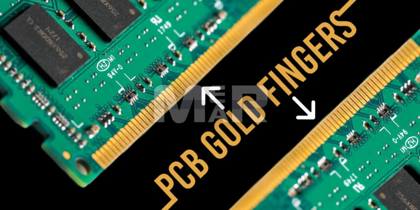
PCB Gold Fingers: Types, Uses, Repairing & Its IPC Standard

In a highly connected world, a big pre-requisite is for the numerous devices that we use, to communicate with each other. This important task is performed by PCB Gold Fingers. They serve as the connection between a secondary PCB to the motherboard of a computer. With the superior connectivity offered by gold, its use is spread across devices that communicate via digital signals.
PCB Gold Fingers
In essence, Gold Fingers are gold plated columns. Looking like fingers this is a long row of PCB pads along the connecting edge of PCBs.
Made out of flesh gold the big advantage that they offer is their superior connectivity. They are also known for their high corrosion resistance and electrical conductivity. The thickness of these Gold Fingers typically ranges between 3 to 50 microns.
YOU MAY ALSO LIKE: Choose right PCB fabrication services
Types of PCB Gold Fingers
Broadly PCB Gold Fingers can be classified into three types:
1. Normal PCB Gold Fingers
These are most commonly used and have an even array. Their PCB pads have the same length, width, and space.
2. Uneven PCB Gold Fingers
Their PCB Pads have the same width but differ in terms of length & spaces.
3. Segmented PCB Gold Fingers
The PCB pads have different lengths. Also, the gold fingers are segmented. These are widely used in many hybrid electronics especially the ones that are water-resistant.
PCB Gold Fingers Beveling
A bevel is created at the edge of the PCB sheet material that ensures PCB insertion in slots.
Angle for PCB gold finger bevel:
Typically, the angle for a PCB gold finger bevel is kept at 45 degrees. However, a 20- and 30-degree bevel is also sometimes preferred. The beveling angle also depends upon the size of the circuit board.
The beveling process involves cutting the edge of the PCB sheet material with the use of automatic beveling equipment. The beveling process is undertaken after the disposition of solder masks. Beveling ensures that the insertions are quicker and effortless.
YOU MAY ALSO LIKE: Silkscreen VS Solder Mask
Essentially the overall plating process comprises of the following steps:
1. Nickel Plating
The connector edges of the fingers are plated with between 3 and 6 microns of nickel.
2. Gold Plating
About 1 to 2 microns of hard gold is plated over the nickel. In turn, the gold is enhanced with cobalt for improved surface resistance
3. Beveling
Typically done at angles of 30 to 45 degrees they help in easier insertion on corresponding slots.
In the plating process some best practices that need to be kept in mind, include:
- Inner layers need to be copper-free along the PCB edge. This will prevent copper exposure during the beveling stage.
- Plated holes, SMD & pads should not be placed within 1 mm of the gold fingers.
- There should be a distance of 0.5 mm between the gold fingers & the outline.
IPC Standard for PCB Gold Finger
Popular standards that are followed in the production of PCB gold fingers, are released by The Association for Connecting Electronics. The earliest standards relating to gold fingers were released in 2002. These were further improved in 2012 & released as the IPC-4556 standards. Of all the standards, the IPC A-600 & IPC-6010 standards of 2015 remain the most popular. Some of the guidelines to manufacture gold fingers include:
1. Chemical Composition
A gold plating consisting of 5 to 10% Cobalt helps in achieving rigidity along the edges of the PCB Gold Fingers.
YOU MAY ALSO LIKE: IPC-6011 Classes
2. Thickness
The thickness of the plating needs to be between 2 to 50 micro inches. The standard thicknesses are:
- 0.031 inches
- 0.062 inches
- 0093 inches
- 0.125 inches
3. Visual Test
A magnifying lens is used to conduct a visual test. It involves checking for smooth contact edges, clean surface as free as no excess plating.
4. Tape Test
It checks the adhesiveness of the gold plating. Essentially, a strip of tape is fastened over the contact edges and is subsequently removed. The tape is then inspected for any traces of plating. In case gold is visible on the tape, the plating is considered insufficient.
Benefits of PCB Gold Fingers
The major advantages that Gold Fingers offer include the following:
- It offers excellent conductivity. The gold in the Gold Fingers helps maintain the necessary connections while also ensuring there is no damage through power use.
- It ensures resistance to wear and tear as the PCB is plugged in and out.
- The hard-gold plating process also lends good oxidation resistance to the PCB pads.
PCB GOLD FINGER REPAIR
Since they are at the periphery of the circuit board, Gold Fingers are prone to damage. Additionally, they are also prone to solder splash during wave soldering. This necessitates restoring the edge contacts to an optimal level of performance. The contaminated contacts are stripped & then replaced by the electroplating process. This ensures functional conductivity as well as durability.
Use of Gold Fingers in PCB
Gold fingers connect PCBs through a strong interlocking system. With gold being highly conductive the power goes through the connectors quickly. Additionally, the use of hard gold also protects the fingers from damage.
Gold Fingers can be used in a wide variety of ways, important among them are:
Interconnected Points
These are the parts of a PCB that connect it to other boards within the computer.
Special Adapters
These connect additional components to the PC structure. Such components include sound card, graphic cards, extra RAM space and more.
External Connections
These are peripherals such as monitors, speakers, and printers. With Gold Fingers high fidelity data transfer is made possible when using these peripherals.
PCB Gold Finger FAQs
1. How much gold is in PCB board?
The gold content in the PCB differs basis the type of PCB & varies between 140 and 700 g of gold for every ton of PCB.
2. What is ENIG finish PCB?
Electroless Nickel Immersion Gold or ENIG refers to a metal plating process. It helps avoid oxidation and improves the solderability of copper contacts as well as plated through-holes.
3. Are traces on PCB gold?
Three commonly used conductive metals include silver, pure copper and pure gold. The importance of the use of gold lies in the fact that it does not oxidize or tarnish. Hard Gold makes for a corrosion resistant and electrically conductive layer. Similarly, gold is also used in Gold Fingers. The gold plating on the edge of conductors protects the conductors from oxidizing & making them more resilient.
We provide cost-effective PCB fabrication and assembly all the while maintaining high-quality standards. Whether you need a small-volume or a high-volume production run our brilliant engineering team strives to reduce the assembly and fabrication costs for our client’s PCBs. We take a custom approach to determine what are the elements that are affecting the cost of production and how they can be tweaked or altered without compromising the functionality and quality of the PCBs.
You can reach out any time and ask our PCB assembly specialists about the quotes that match your budgetary targets. You may also contact our manager to review your quote and find out the cost-reducing options.
Get a quick PCB fabrication quote!


